Tech 101 From Symmetry Electronics: What's a PCB?

About Symmetry Electronics Team
Established in 1998, Symmetry Electronics is a focused global distributor of wireless connectivity solutions, sensors, and audio-video technologies. Offering comprehensive design support and available-to-ship inventory, Symmetry is committed to helping engineers accelerate time to market, reduce costs, and offer modern solutions for their IoT designs. Acquired by Berkshire Hathaway company, TTI, Inc. in 2017, Symmetry Electronics is part of the Exponential Technology Group (XTG) – a supergroup of electronic component distributors and engineering services firms working together to advance the electronics industry. For more information, visit www.symmetryelectronics.com.
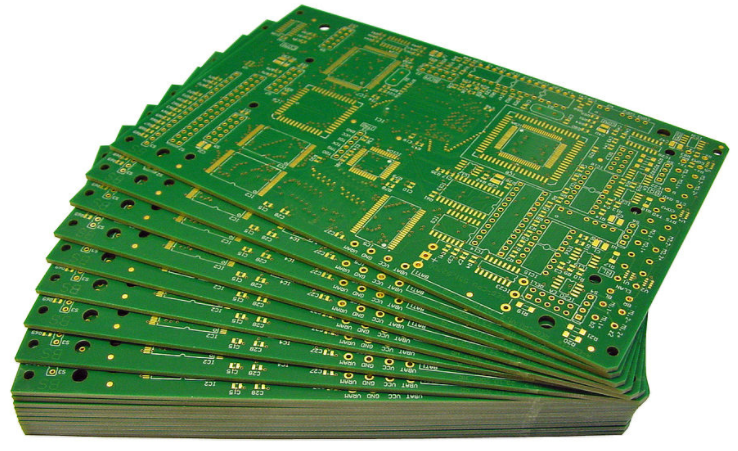
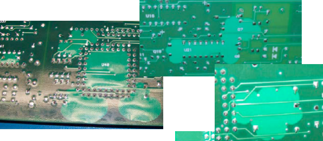
A Printed Circuit Board (PCB) mechanically supports and electrically connects electronic components using conductive tracks. It is etched from copper sheets which are then laminated onto a non-conductive substrate (usually fiberglass). Rigid PCBs or hardboards are the most common type of PCB and what is implemented on nearly all the modules we sell.
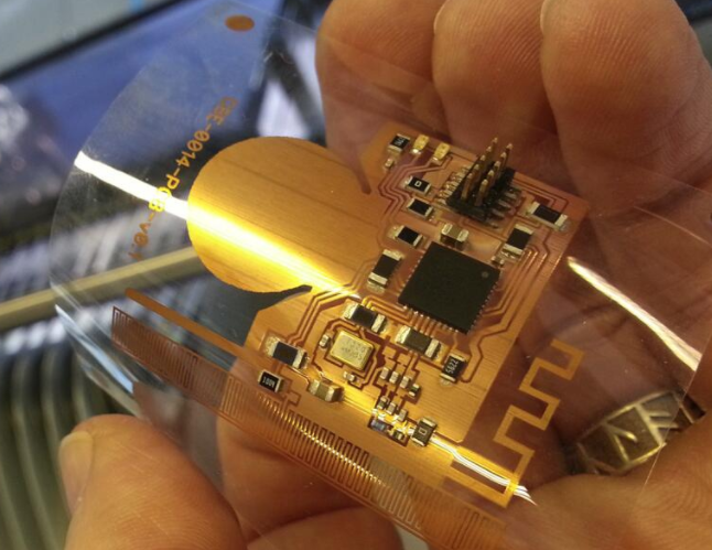
The term PCB is synonymous with rigid PCBs although in recent years, Flex circuits (flexible PCBs) have become more popular- especially with the boom in wearables. With flex circuits, a flexible substrate is used to support all components and traces- it can bend, fold and twist where a rigid PCB cannot.
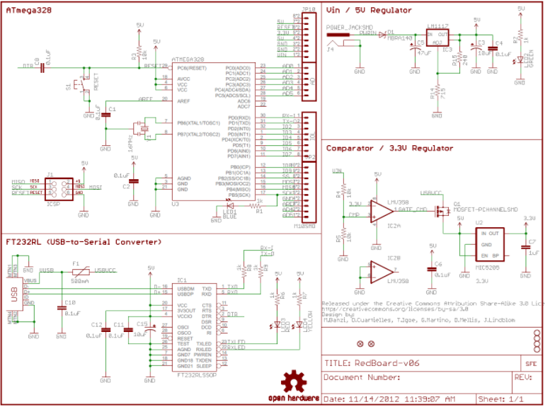
When designing an electrical device, circuit designers start with a schematic of their design.
This is a blueprint for their intended design containing all components and connection points.
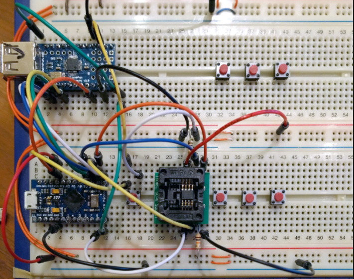
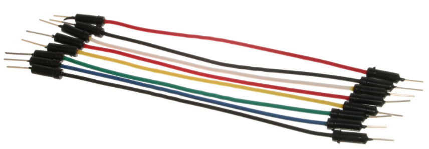
Once they have created a schematic, typically the design is implemented and tested using a breadboard. A breadboard is a construction base for prototyping of electronics. Columns of holes are electrically connected (under the plastic) so that all components from the schematic can be placed on the breadboard without the need for tedious soldering. To connect the nodes from two components, a jumper wire is easily pressed into the breadboard ensuring a secure connection between the two points. Breadboards have limitations compared to soldering wires- you can read more about the pros and cons of breadboards at a link located at the end of this document.
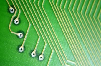
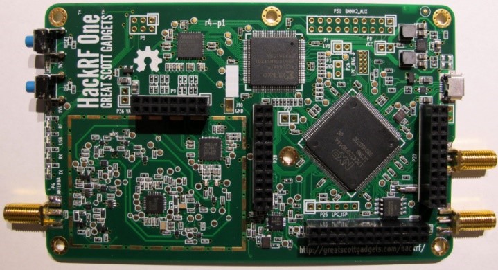
Once the design is working with a breadboard and the schematic is proven to be working and correct, circuit designers move onto a PCB. A PCB is a slimmed down version of the breadboard circuit. It has traces instead of wires, and all the components are soldered to these traces. You can think of PCB traces as nothing more than very thin, flat wires etched out of copper substrate on the top of the board.
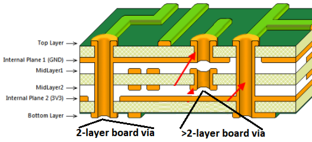
PCBs can come in single or multiple layer boards. In general, unless the design is very simple, a PCB has two or more layers. Multiple layers are necessary when two traces (wires) must cross. Because the traces are all on the same plane, and a trace cannot “jump” over another trace, a via is implemented. A via is a physical hole drilled into the PCB substrate with solder mask inserted into the hole. This solder mask connects the traces between each layer of the board, and allows a trace to “jump” to the other side of the board and then back over again once it is past the trace that it is intersecting with. Boards with more than 2 layers have make this jump to another plane sandwiched between the top and bottom planes.
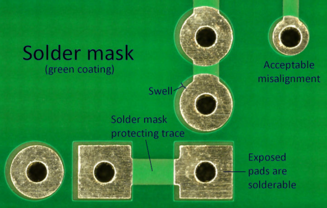
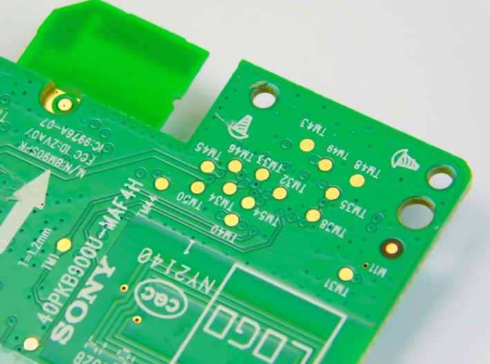
When a PCB is created, and the copper layer has been etched away everywhere besides where the traces are, at this point solder mask is applied to the top of the board. Solder mask is a thin lacquer-like layer of polymer that is applied to the board everywhere besides where components will be soldered to. Applying solder mask protects the traces again oxidation and prevents solder bridges from forming between closely spaced solder pads.
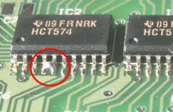
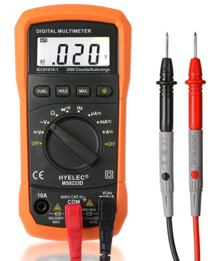
In some designs, test points are added- test points enable debugging of the PCB hardware. Because all the traces are covered with solder mask, a multimeter (or some other measuring instrument) cannot make direct electrical contact with the trace. A test point is a copper pad broken out from a trace which does not have solder mask on it. This pad allows a multimeter to make direct contact with the trace and provides more area of contact than a thin trace would. A multimeter is an instrument designed to measure electric current, voltage, and resistance. Typically, the measured values are displayed on a digital gauge.
Sometimes a connection between components on a PCB are unwanted. This may be due to an error in schematic and PCB, or because a change needs to be made from the intended PCB’s application. When this occurs, you can’t just snip the wire, because all the wires (traces) are fixed to the board. Instead, a trace is cut, usually with a sharp knife.
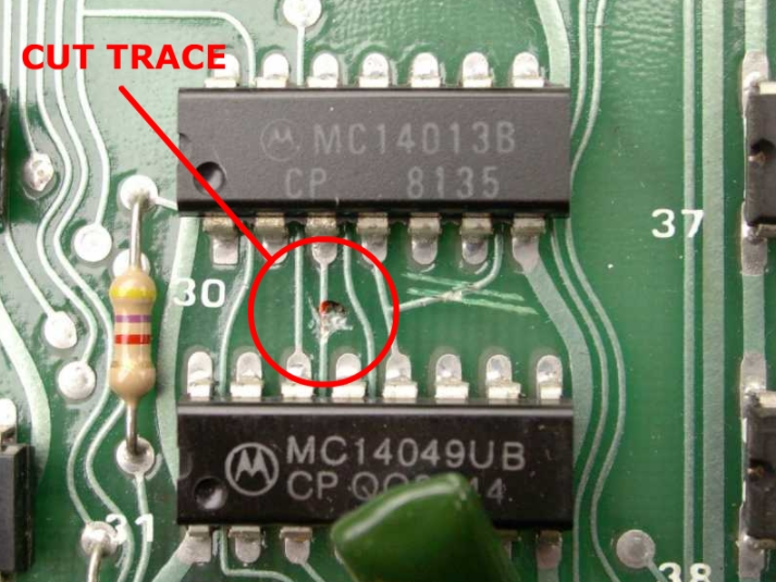
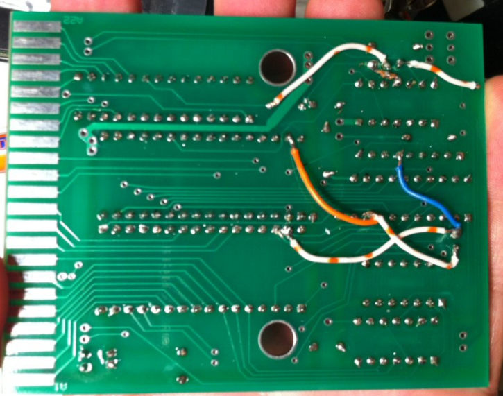
Similarly, if a wire needs to be added to a PCB after it is manufactured, a jumper wire can be soldered in place. Generally, PCB cuts and jumpers are added in the prototyping phase and not after production.
Sometimes PCBs experience delamination well after they have been produced and are sitting in inventory or out in a product. Delamination is a separation of solder mask (laminate), traces or pads from the substrate they are mounted to. This can occur if the PCB manufacturer is using laminates that don’t adhere to specification or if the PCB is exposed to moisture. PCBs that experience delamination can fail as traces break and components become unsoldered.
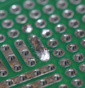
Another issue that PCBs might experience is something called a cold solder joint. Solder, when it is melted to connect components and traces, must not be moved while the solder is solidifying. If the solder is moved or not hot enough to begin with, then there is not a solid connection between whatever the solder is attempting to connect. Cold solder joints may go unnoticed as a circuit will still function as expected during testing. As a PCB is exposed to temperature change, vibrations and humidity over time, these cold solder joints may fail rendering the entire circuit defective. Cold solder joints may appear frosted, crystalline or rough.
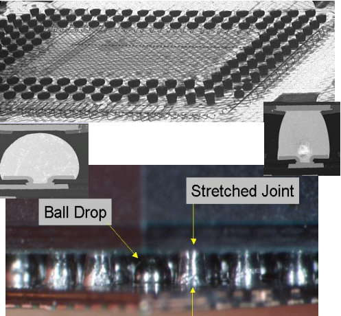
Last but certainly not least is a PCB issue known as warpage. Warpage can occur for any number of reasons usually during the PCB baking process. When a PCB is populated with ICs, solder is applied to the contacts and the entire board is heated up to melt the solder and physically connect the ICs to the PCB. During the PCB manufacturing process, if the rigid substrate is too thin and not within specification, it may warp or bend during the baking process. Solder may also have to stretch to reach each contact point, or not reach at all. Non-uniform heating and cooling or unbalanced board design can also cause warpage to occur.
Additional Resources:
Printed circuit board vs flex circuits
What is delamination
Root cause failure analysis of printed circuit board assemblies

About Symmetry Electronics Team
Established in 1998, Symmetry Electronics is a focused global distributor of wireless connectivity solutions, sensors, and audio-video technologies. Offering comprehensive design support and available-to-ship inventory, Symmetry is committed to helping engineers accelerate time to market, reduce costs, and offer modern solutions for their IoT designs. Acquired by Berkshire Hathaway company, TTI, Inc. in 2017, Symmetry Electronics is part of the Exponential Technology Group (XTG) – a supergroup of electronic component distributors and engineering services firms working together to advance the electronics industry. For more information, visit www.symmetryelectronics.com.